


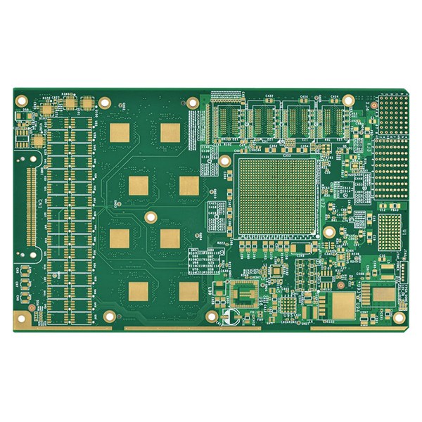
Multilayer PCB assembly is the process of building and populating circuit boards that contain three or more conductive copper layers stacked inside a single board. While a simple board has copper on only its top and bottom surfaces, a multilayer board hides additional signal, power, and ground layers between them. This structure allows far more connections in a smaller footprint, which is why multilayer boards power smartphones, computers, medical devices, and industrial control systems. Assembly of these boards demands careful handling, because the complexity is built into the board long before any component is placed.
The stackup is the blueprint of a multilayer board. It defines the order of copper layers and insulating materials, the thickness of each layer, and how the layers connect. A typical four-layer board places signal layers on the outside with power and ground planes inside, giving signals a clean reference and reducing interference. Boards with six, eight, or more layers follow the same idea at greater density, with dedicated layers for high-speed signals, controlled impedance, and power distribution. Getting the stackup right is essential for both electrical performance and reliable assembly.
Fabrication of a multilayer board begins with imaging and etching the inner layers, which are then laminated together under heat and pressure with insulating prepreg material. Alignment during lamination must be extremely accurate, because a shift of even a fraction of a millimetre can break connections between layers. After lamination, holes are drilled through the stack and plated with copper, creating the vias that carry signals from one layer to another. The finished bare board is then inspected to confirm that every layer is correctly registered before assembly begins.
Vias are one of the defining features of multilayer PCB assembly. Through vias pass through the whole board, while blind vias connect an outer layer to an inner layer and buried vias connect inner layers only. These different via types let designers route dense circuits without wasting surface space. However, they also add fabrication steps and cost, and they affect how the board behaves during soldering. Assembly engineers must know the via structure to choose the right soldering profile and to avoid defects such as trapped air or cracked plated holes.
Surface mount assembly on a multilayer board follows the same core steps as on simpler boards, but with tighter tolerances. Solder paste is printed, components are placed by machine, and the board passes through a reflow oven where the paste melts and forms joints. Because multilayer boards are thicker and contain large copper planes, they absorb and spread heat differently, so the reflow profile must be tuned to heat the board evenly. Uneven heating can cause tombstoning, poor wetting, or stress on the board, so thermal profiling is a routine part of quality multilayer assembly.
Power integrity is a major advantage of multilayer construction. Dedicated power and ground planes deliver stable voltage to every part of the board and provide a low-impedance return path for signals. This reduces noise, limits voltage drop, and helps high-speed circuits behave predictably. During assembly, good power integrity also means that large ground planes can act as heat sinks, which is helpful for cooling but must be managed during soldering. Designers balance these effects by choosing plane sizes, copper weights, and thermal relief patterns that serve both electrical and assembly needs.
Signal integrity is equally important in multilayer PCB assembly. High-speed signals are sensitive to the distance between a trace and its reference plane, so controlled impedance routing is used to keep signal quality consistent. The stackup, trace width, and dielectric material all influence impedance, and assembly must preserve the design by avoiding damage to the board surface or incorrect component placement. Testing after assembly often includes checking high-speed interfaces with real signals, because a board that looks perfect can still fail if a signal path is degraded.
Inspection of assembled multilayer boards uses several complementary methods. Automated optical inspection checks component placement and visible solder joints, while X-ray inspection is especially valuable because it reveals hidden joints under large packages and confirms that vias are intact. Electrical testing verifies that every net connects as designed and that no shorts exist between layers. For critical applications, cross-section analysis of sample boards can confirm plating quality and layer alignment, giving further confidence in the manufacturing process.
Thermal management deserves special attention in multilayer PCB assembly. Dense boards with powerful processors, power converters, or radio circuits generate significant heat, and the internal copper planes can either help spread that heat or trap it, depending on the design. Thermal vias carry heat from hot components to cooler layers, and careful component placement keeps heat sources away from temperature-sensitive parts. Assembly processes must respect the board’s thermal limits, because repeated or excessive heating can weaken the laminate and reduce long-term reliability.
Design challenges in multilayer boards are mostly about density and discipline. With many layers available, it is tempting to route freely, but every additional layer adds cost and manufacturing risk. Good designers use only as many layers as the circuit truly needs, keep high-speed and sensitive signals separated, and leave room for test points and rework. Clear documentation of the stackup, materials, and assembly notes prevents misunderstandings between design and manufacturing teams and keeps the project on schedule.
Applications for multilayer PCB assembly span almost every modern industry. Consumer electronics use them to pack more features into thinner devices, automotive systems rely on them for engine controllers and driver assistance, medical equipment depends on their reliability for monitoring and imaging, and telecommunications hardware needs them for high-speed data paths. In each case, the same qualities matter: compact size, stable power, clean signals, and a board that survives years of use in its intended environment.
Choosing a partner for multilayer PCB assembly means looking for proven experience with complex boards. The right partner reviews the stackup before fabrication, confirms that via structures and materials are manufacturable, and uses inspection methods suited to hidden joints. Transparent communication about lead times, yields, and test results helps customers plan with confidence. Multilayer assembly rewards preparation and precision, and the boards it produces form the hidden backbone of the electronic products people rely on every day.
